Applications
- Surface roughness measurement
- Wafer defects inspection
- Local electrical properties measurement
- Thin films and coating thicknesses measurement
- Elastic properties study
- Etching depth control
A lot of nondestructive testing methods on a single platform for comprehensive analysis of Ø300 mm wafers
The development of semiconductor wafer industry requires to control reliably geometric, mechanical, chemical, and electrophysical parameters at the production steps. The testing, the detection and the elimination of defects on time are necessary to accelerate the manufacturing process.
The combination of various analysis methods within a single device leads to the entire production process optimization. Despite the variety of inspection methods, profilometry remains the very popular one.
Profilometry is a technique used to measure the surface profile. It yields information on surface morphology, step heights and surface roughness. In general, profilometry techniques are divided into contact and optical ones, both of them have some benefits.
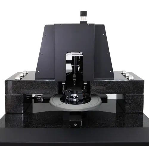
The uSTEP 300 is a universal platform with functional modules combining different profilоmetry regimes inside one instrument. Based on the uSTEP 300 both contact and non-contact methods of roughness analysis, and analysis of electrical, physical and chemical surface properties for large samples (up to 300 mm in diameter) with various roughness can be realized.
The uSTEP 300 is equipped with a scanning stage with the lateral positioning accuracy up to 25 nm, allowing 3D maps to be acquired automatically from the defined areas.
The unique design of the uSTEP 300 profilometer allows to work with samples up to 20 mm in thick and 25 - 300 mm in diameter. Vacuum wafer fixation and built-in vibration isolation by pneumatic supports reduce the influence of mechanical noise.
Monolithic design of the profilometer base reduces the parasitic noise by 30 dB in the frequency bandwidth above 200 Hz. For additional vibration impact minimization, the system can be equipped with an active vibration isolation module operating in the frequency range of 1-200 Hz with a response time of about 0.5 ms.
The software automatically acquires and analyzes the data obtained. uSTEP 300 is controlled by the Nova SPM program installed on Windows 10, 11.
The intuitive software design allows to work both in a simplified mode for quick surface roughness analysis and in an advanced mode for more detailed and complex research of the sample features automatically.
Built-in data processing package makes available a variety of useful operations, including the wafer curvature and roughness characterization, and 3D mapping of the sample surface. The data obtained can be processed by third-party software packages (MS Excel, Origin). Users can additionally utilize their own script procedures for the unique tasks.
Due to the modular design of the uSTEP 300 profilometer, its separate units can be successfully used in the microelectronics fab lines. The development of fab modules with uSTEP 300 integrated in is possible also in cooperation with the leading industry and research teams.
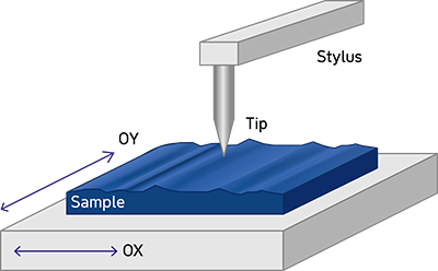
The principle of stylus profilometer operation is based on keeping constant force applied to the sample surface by the stylus (probe). Passing over the surface, the stylus deflection restores its profile.
With a number of consecutively measured profiles, it is possible to reconstruct the surface 3D image. By choosing the probe (the probe curvature radius can be from tens of micrometers to submicrometers), it is possible to control the precision of measurements.
This method of analysis provides fast routine measurements of materials with a low-roughness surface.
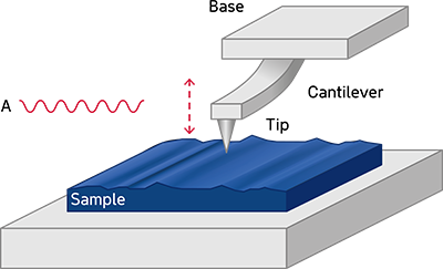
An Atomic-Force Microscope (AFM) and a profilometer both use sharp tips to study the surface morphology.
However, the AFM tip curvature radius is of a nanometer scale, which allows to study the sample in more detail. In addition, the use of semi-contact AFM mode significantly reduces mechanical interaction between the probe and the sample, preventing the possible deformation of them.
Different AFM modes in combination supply additional information of local mechanical (stiffness, adhesion, Young's modulus, etc.), electrical (conductivity, capacitance, surface potential, etc.), and magnetic features of the sample surface.
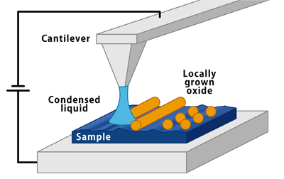
Based on scanning probe microscopy techniques, the atomic force nano-lithograph enables to create pre-designed structures with spatial resolution up to 10 nm without using masks. The software supports both raster and vector lithography capabilities. The lithography templates can be either generated manually using software tools or uploaded from outside. AFNL supports various types of lithography: mechanical, electrical, etc.
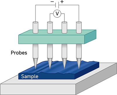
To characterize the sample surface better in terms of its electrophysical properties, the uSTEP 300 profilometer uses traditional four-probe method of measuring surface resistance, which can be especially useful while studying various conductive materials.
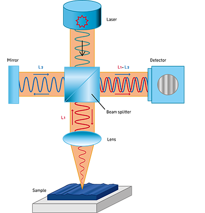
Non-contact methods for surface roughness investigation include optical profilometry, which uses optical “probe” instead of a mechanical probe.
The optical interferometer head inside uSTEP 300 includes a beamsplitter and a mirror to create an interferometric pattern, which is captured by a photo detector to control the beam path difference and, consequently, the head position height above the surface under investigation.
The main advantages of this method are: fast measurements, no mechanical contact with the surface, no sample material damage.
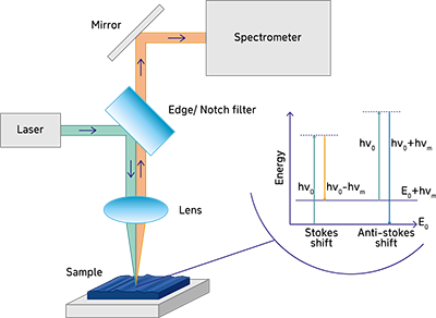
Using the uSTEP 300 profilometer, the surface roughness mapping and the chemical composition analysis can be done simultaneously by combining mechanical probe and optical analysis.
The instrument is equipped with a spectrometer, enabling fast local measurements of Raman spectra, PL spectra, light scattering, etc.
The “Raman-probe” configuration can use lasers with different wavelengths: 405, 532, 633, and 785 nm.
| XY sample positioning | Positioning sensors resolution | 25 nm |
| Positioning rate | 4 mm/s | |
| Sample stage with vacuum holder | Sample size | ø 25 – 300 mm ø 1 – 12“ |
| AFM scanning head with piezo scanner | Scan range | 60 × 60 × 7 µm |
| AFM deflectometer | Laser wavelength | 650 nm/ 830 nm |
| Photodetector | Quadrant photodiode | |
| Optical microscopy head | Objectives | 10х, 50х |
| Raman spectra analyzer (option) | “Raman-probe”, fiber type Excitation laser λ = 405/532/633/785 nm Monochromator with focal length 620 mm, spectral resolution ≤ 1 cm⁻¹ CCD camera |
|
| Base frame with passive vibration isolation | Material | Gabbro-diabase |
| Active* vibration isolation | Frequency bandwidth | 1 – 200 Hz |
| Vibration isolation performance | - 40 dB at 70 Hz | |
| Thermal stability | Active temperature control | PID |
| Internal temperature stability at the ambient temperature variation by 1°C | < 0.05 °С | |
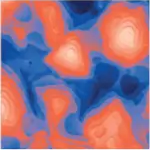
BiSbTeSe2 epitaxial film on Si;
AFM image.
Scan size: 2x2 µm
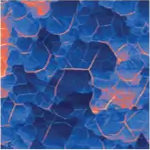
Carbon sample.
Kelvin probe mode with amplitude modulation.
Scan size: 10x10 µm
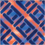
Si microstructure;
AFM image. Phase contrast.
Scan size: 50x50 µm
SiC steps with a height of 1.5 nm.
Semi-contact AFM image.
Scan size: 3x3 µm